- 您现在的位置:买卖IC网 > Sheet目录322 > DS28CZ04G-4+T (Maxim Integrated)IC EEPROM 4KBIT 400KHZ 12TQFN
DS28CZ04: 4Kb I2C/SMBus EEPROM with Nonvolatile PIO
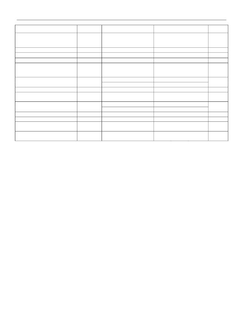
PARAMETER
SYMBOL
CONDITIONS
MIN
TYP
MAX
UNITS
Input Current with an Input
Voltage Between 0.1V CC and
0.9V CCmax
Input Capacitance
SCL Clock Frequency
Bus Time-Out
I I
C I
f SCL
t TIMEOUT
(Note 11)
(Notes 5, 9)
(Note 12)
(Note 12)
-10
25
10
10
400
75
μA
pF
kHz
ms
Hold Time (Repeated) START
Condition. After this Period, the
First Clock Pulse is Generated.
LOW Period of the SCL Clock
(Note 13)
HIGH Period of the SCL Clock
Setup Time for a Repeated
START Condition
t HD:STA
t LOW
t HIGH
t SU:STA
(Note 13)
V CC ≥ 2.7V
V CC < 2.7V
(Note 13)
(Note 13)
0.6
1.3
1.5
0.6
0.6
μs
μs
μs
μs
Data Hold Time (Notes 14, 15)
t HD:DAT
V CC ≥ 2.7V
V CC < 2.7V
0.3
0.3
0.9
1.1
μs
Data Setup Time
Setup Time for STOP Condition
Bus Free Time Between a
STOP and START Condition
Capacitive Load for Each Bus
Line
t SU:DAT
t SU:STO
t BUF
C B
(Notes 13, 16)
(Note 13)
(Note 13)
(Notes 5, 13)
100
0.6
1.3
400
ns
μs
μs
pF
Note 1:
Note 2:
Note 3:
Note 4:
Note 5:
Note 6:
Note 7:
Note 8:
Note 9:
Note 10:
Note 11:
Note 12:
Note 13:
Note 14:
Note 15:
Note 16:
Specifications at -40 ° C are guaranteed by design and characterization only and not production tested.
To the first order, this current is independent of the supply voltage value.
All PIO are tri-stated at beginning of reset prior to setting to Power-On values.
This specification is valid for each 16-byte memory block.
Not production tested. Guaranteed by design or characterization.
EEPROM writes can become nonfunctional after the data-retention time is exceeded. Long-time
storage at elevated temperatures is not recommended; the device can lose its write capability after 10
years at +125°C or 40 years at +85°C.
All values are referenced to V IHmin and V ILmax levels.
The maximum specification value is guaranteed by design, not production tested.
Applies to SDA and SCL.
C B = total capacitance of one bus line in pF. If mixed with HS-mode devices, faster fall-times according
to I2C-Bus Specification v2.1 are allowed.
The DS28CZ04 does not obstruct the SDA and SCL lines if V CC is switched off.
The minimum SCL clock frequency is limited by the bus timeout feature. If the CM bit is 1 AND SCL
stays at the same logic level or SDA stays low for this interval, the DS28CZ04 behaves as though it
has sensed a STOP condition.
System Requirement
The DS28CZ04 provides a hold time of at least 300ns for the SDA signal (referred to the V IHmin of the
SCL signal) to bridge the undefined region of the falling edge of SCL.
The maximum t HD:DAT has only to be met if the device does not stretch the low period (t LOW ) of the SCL
signal.
A Fast-mode I2C-bus device can be used in a standard-mode I2C-bus system, but the requirement
t SU:DAT ≥ 250ns must then be met. This is automatically the case if the device does not stretch the LOW
period of the SCL signal. If such a device does stretch the LOW period of the SCL signal, it must
output the next data bit to the SDA line t rmax + t SU:DAT = 1000 + 250 = 1250ns (according to the
standard-mode I2C-bus specification) before the SCL line is released.
3 of 22
发布紧急采购,3分钟左右您将得到回复。
相关PDF资料
DS28DG02E-3C+T
IC EEPROM 2KBIT 2MHZ 28TSSOP
DS28E04S-100+T
IC EEPROM 4KBIT 16SOIC
DS28EC20+T
IC EEPROM 20KBIT TO92-3
DS301X
KWIK-CHG DESIGNATION STRIP SGL
DS3030W-100#
IC NVSRAM 256KBIT 100NS 256BGA
DS3045W-100#
IC NVSRAM 1MBIT 100NS 256BGA
DS3050W-100#
IC NVSRAM 4MBIT 100NS 256BGA
DS3065W-100#
IC NVSRAM 8MBIT 100NS 256BGA
相关代理商/技术参数
DS28D02S-FA00
功能描述:电可擦除可编程只读存储器
RoHS:否 制造商:Atmel 存储容量:2 Kbit 组织:256 B x 8 数据保留:100 yr 最大时钟频率:1000 KHz 最大工作电流:6 uA 工作电源电压:1.7 V to 5.5 V 最大工作温度:+ 85 C 安装风格:SMD/SMT 封装 / 箱体:SOIC-8
DS28D02S-FA00+
功能描述:电可擦除可编程只读存储器
RoHS:否 制造商:Atmel 存储容量:2 Kbit 组织:256 B x 8 数据保留:100 yr 最大时钟频率:1000 KHz 最大工作电流:6 uA 工作电源电压:1.7 V to 5.5 V 最大工作温度:+ 85 C 安装风格:SMD/SMT 封装 / 箱体:SOIC-8
DS28DG02
制造商:DALLAS 制造商全称:Dallas Semiconductor 功能描述:2kb SPI EEPROM with PIO, RTC, Reset, Battery Monitor, and Watchdog
DS28DG02E-3C+
功能描述:电可擦除可编程只读存储器 2Kb SPI 电可擦除可编程只读存储器 w/PIO RTC/Rst/Bat Mtr/Wtdg RoHS:否 制造商:Atmel 存储容量:2 Kbit 组织:256 B x 8 数据保留:100 yr 最大时钟频率:1000 KHz 最大工作电流:6 uA 工作电源电压:1.7 V to 5.5 V 最大工作温度:+ 85 C 安装风格:SMD/SMT 封装 / 箱体:SOIC-8
DS28DG02E-3C+T
功能描述:电可擦除可编程只读存储器 2Kb SPI 电可擦除可编程只读存储器 w/PIO RTC/Rst/Bat Mtr/Wtdg RoHS:否 制造商:Atmel 存储容量:2 Kbit 组织:256 B x 8 数据保留:100 yr 最大时钟频率:1000 KHz 最大工作电流:6 uA 工作电源电压:1.7 V to 5.5 V 最大工作温度:+ 85 C 安装风格:SMD/SMT 封装 / 箱体:SOIC-8
DS28DG02EVKIT
功能描述:存储器 IC 开发工具 RoHS:否 制造商:STMicroelectronics 产品:Reference Boards 工具用于评估:M24LR64-R 存储容量:64 kbit 存储类型:EEPROM 工作电源电压:1.8 V to 5.5 V
DS28DG02G-3C+
功能描述:电可擦除可编程只读存储器 2Kb SPI 电可擦除可编程只读存储器 w/PIO RTC/Rst/Bat Mtr/Wtdg RoHS:否 制造商:Atmel 存储容量:2 Kbit 组织:256 B x 8 数据保留:100 yr 最大时钟频率:1000 KHz 最大工作电流:6 uA 工作电源电压:1.7 V to 5.5 V 最大工作温度:+ 85 C 安装风格:SMD/SMT 封装 / 箱体:SOIC-8
DS28DG02G-3C+T
功能描述:电可擦除可编程只读存储器 2Kb SPI 电可擦除可编程只读存储器 w/PIO RTC/Rst/Bat Mtr/Wtdg RoHS:否 制造商:Atmel 存储容量:2 Kbit 组织:256 B x 8 数据保留:100 yr 最大时钟频率:1000 KHz 最大工作电流:6 uA 工作电源电压:1.7 V to 5.5 V 最大工作温度:+ 85 C 安装风格:SMD/SMT 封装 / 箱体:SOIC-8
